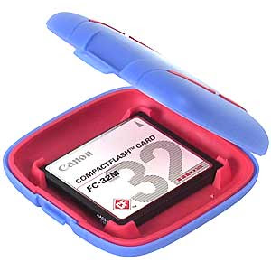
 Flash memory technology is a mix of EPROM and EEPROM technologies. The term “flash” waschosen because a large chunk of memory could be erased at one time. The name, therefore, dis-tinguishes flash devices from EEPROMs, where each byte is erased individually.
Flash memory technology is today a mature technology. It is a strong competitor to other non-volatile memories such as EPROMs and EEPROMs, and to some DRAM applications.
HOW THE DEVICE WORKS
The more common elementary flash cell consists of one transistor with a floating gate, similar to an EPROM cell. However, technology and geometry differences between flash devices and EPROMs exist. In particular, the gate oxide between the silicon and the floating gate is thinner for flash technology.Source and drain diffusions are also different. These differences allow the flash device to be programmed and erased electrically. Comparison between a flash memory cell and anEPROM cell from a same manufac-turer (AMD) with the same technol-ogy complexity. The cells look similar since the gate oxide thick-ness and the source/drain diffusion differences are not visible in the photographs.
The electrical functionality of the flash memory cell is similar to that of an EPROM or EEPROM. Electrons are trapped onto the floating gate. These elec-trons modify the threshold voltage of the storage transistor. Electrons are trapped in the floating gate using Fowler-Nordheim tunneling (as with the EEPROM) or hot electron injection (as with the EPROM). Electrons are removed from the floating gate using Fowler-Nordheim tunneling as with the EEPROM.
ARCHITECTURE
As with other semiconductors, the flash memory chip size is the major contributor to the cost of the device. For this reason, designers have developed alternative memory array architectures,yielding a trade-off between die size and speed. NOR, NAND, DINOR, and AND are the main architectures developed for flash memories.
NOR Cell
The NOR architecture is currently the most popular flash architecture. It is commonly used inEPROM and EEPROM designs. Aside from active transistors, the largest contributor to area in the cell array is the metal to diffusion contacts. NOR architecture requires one contact per two cells,which consumes the most area of all the flash architecture alternatives. Electron trapping in thefloating gate is done by hot-electron injection. Electrons are removed by Fowler-Nordheim tunnel-ing. The world’s leading manufacturers of flash devices (Intel, AMD) use NOR cell configurations.
PCMCIA
Magnetic memory storage and flash memory devices will co-exist. Magnetic memory will con-tinue to dominate in ultra-high capacity, low cost/Mbyte applications where power, weight/size,and mechanical ruggedness are not a consideration. Flash-based mass storage will become per-vasive in small, low power, portable electronic platforms, providing low power, small size, andunparalleled ruggedness/reliability and offering lowest entry cost of any mass storage. PCMCIA(Personal Computer Memory Card International Association) cards were developed for this flashmass storage application.
CompactFlash
CompactFlash was developed by SanDisk Corporation, Sunnyvale, California, in 1994. TheCompactFlash Association (CFA) was established in October, 1995, to promote and encourage theworldwide adoption of CompactFash technology as an open industry standard. More than 40companies have joined the CFA.
The CompactFlash design incorporates the ATA (AT-Attachment) interface standard, that uses thesame electrical signals as PCMCIA/ATA flash cards. The first product that employedCompactFlash technology was IBM’s Palm Top PC110, which was introduced in September, 1995.
Miniature Card
The Miniature Card, originally developed by Intel, is supported by the Miniature Card Implementers Forum (MCIF). The Miniature Card incorporates a linear-addressed format likePCM CIAflash cards. This card needs host-based software to be read. This software is called Flash Translation Layer (FTL) and was developed by M Systems. Miniature Cards are cheaper than CompactFlash cards but need that additional software. ATA configuration versus the linear configuration. Intel developed its Miniature Card for high-volume consumer applications and will not support CompactFlash.
RELIABILITY CONCERNS
There are three primary reliability concerns of a flash memory IC. They are data retention, thin oxide stress, and over or under erasing/programming.
Regarding erase/program, flash ICs that use hot electron injection for trapping electrons in thefloating gate are programmed (data equal to 0) by capturing electrons in the floating gate, as withan EPROM.
Flash ICs that use Folwer-Nordheim tunneling for trapping electrons in the floating gate will beprogrammed (data equal to 0) by removing the electrons from the floating gate, as with anEEPROM. The reliability concern is to either over program or over erase.
Also See..


No comments:
Post a Comment